

A | B | C | D | E | F | G | H | CH | I | J | K | L | M | N | O | P | Q | R | S | T | U | V | W | X | Y | Z | 0 | 1 | 2 | 3 | 4 | 5 | 6 | 7 | 8 | 9

Eredeti fájl (SVG fájl, névlegesen 723 × 524 képpont, fájlméret: 32 KB)
|
Ez a fájl a Wikimedia Commonsból származik. Az alább látható leírás az ottani dokumentációjának másolata. A Commons projekt szabad licencű kép- és multimédiatár. Segíts te is az építésében! |
Összefoglaló
| Leírás |
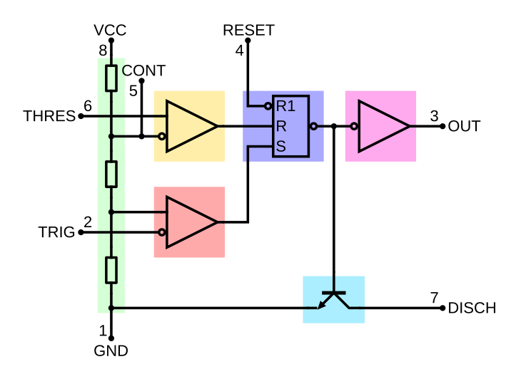
English: The NE555 contains 24 bipolar transistors, two diodes and 15 resistors that form six functional blocks:
Between the supply voltage VCC (+) and the ground GND (-) is a voltage divider consisting of three identical resistors which, when connected not from the outside, the two reference voltages ¹ / 3 VCC and ² / 3 VCC supplies. The latter is at the terminal pin Control Voltage available. The block diagram and schematic that area is highlighted in green. Two comparators are each connected to one of the reference voltages, while the other two inputs of which are fed directly to the terminals of trigger or threshold. The block diagram in yellow and orange. A flip-flop, deposited in the color purple, stores the state of the timer and is controlled by the two comparators. Via the reset terminal overrides the other two inputs, the flip-flop (and therefore the entire timer device) be reset at any time. At the output of flip-flop followed by an output stage with totem-pole output that can be loaded at the port output with up to 200 mA. Shown in the color pink. Parallel to the output stage of a transistor is connected, the collector is located on the discharge port. The transistor in the circuit diagram is a light blue background, always energized when the output is low level.Deutsch: Der NE555 enthält 24 Bipolartransistoren, zwei Dioden und 15 Widerstände, die zusammen sechs Funktionsblöcke bilden:
|
| Dátum | |
| Forrás | A feltöltő saját munkája |
| Szerző | BlanchardJ |
| Más változatok |
  |
Licenc
| Én, a szerző, ezt a művemet ezennel közkinccsé nyilvánítom. Ez a világ minden részén érvényes. Egyes országokban ez jogilag nem lehetséges. Ha így van, akkor: Jogot adok bárkinek, hogy bármilyen célból, feltétel nélkül használhassa ezt a fájlt, kivéve a törvény által kötelezően előírt feltételeket. |
Fájltörténet
Kattints egy időpontra, hogy a fájl akkori állapotát láthasd.
| Dátum/idő | Bélyegkép | Felbontás | Feltöltő | Megjegyzés | |
|---|---|---|---|---|---|
| aktuális | 2012. január 16., 21:54 | | 723 × 524 (32 KB) | Wdwd | Colored function blocks (for circiut diagram) correct transistor symbol (without a circle, because it's inside the chip) |
| 2009. június 8., 01:27 |  | 723 × 524 (40 KB) | Brighterorange | remove spurious red dot | |
| 2007. szeptember 23., 22:22 |  | 723 × 524 (40 KB) | BlanchardJ | {{Information |Description=Bloc diagram of a 555 timer IC |Source=self-made |Date=September 23 2007 |Author=BlanchardJ |Permission= |other_versions= }} {{Created with Inkscape}} {{ElCompLib}} Category:555 timer IC |
Fájlhasználat
Az alábbi lap használja ezt a fájlt:
Globális fájlhasználat
A következő wikik használják ezt a fájlt:
- Használata itt: ar.wikipedia.org
- Használata itt: beta.wikiversity.org
- Használata itt: ca.wikipedia.org
- Használata itt: cs.wikipedia.org
- Használata itt: cs.wikibooks.org
- Használata itt: de.wikipedia.org
- Használata itt: en.wikipedia.org
- Használata itt: es.wikipedia.org
- Használata itt: et.wikipedia.org
- Használata itt: fa.wikipedia.org
- Használata itt: fi.wikipedia.org
- Használata itt: fr.wikipedia.org
- Használata itt: fr.wikiversity.org
- Használata itt: he.wikipedia.org
- Használata itt: hi.wikipedia.org
- Használata itt: id.wikipedia.org
- Használata itt: it.wikipedia.org
- Használata itt: ja.wikipedia.org
- Használata itt: lt.wikipedia.org
- Használata itt: no.wikipedia.org
- Használata itt: pl.wikipedia.org
- Használata itt: pt.wikipedia.org
- Használata itt: ru.wikipedia.org
- Használata itt: uk.wikipedia.org
- Használata itt: vi.wikibooks.org
- Használata itt: zh.wikipedia.org
Metaadatok
A lap szövege Creative Commons Nevezd meg! – Így add tovább! 3.0 licenc alatt van; egyes esetekben más módon is felhasználható. Részletekért lásd a felhasználási feltételeket.
Analóg multiméterek túlterhelés elleni védelme
Egyenáram
Egyenáram mérése
Egyenirányítós lengőtekercses műszer
Elektromágnes (fizika)
Elektromos feszültség
Elektromos térerősség
Fáziseltolódás
Fázismutató
Fajlagos ellenállás
Feszültséggenerátor
Feszültségváltó
Forgó mágneses tér
Háromfázisú hálózat
Hőelektromosság
Hatásos ellenállás
A lap szövege Creative Commons Nevezd meg! – Így add tovább! 3.0 licenc alatt van; egyes esetekben más módon is felhasználható. Részletekért lásd a felhasználási feltételeket.